Simplify the Design of Secure Line-Powered Smart Devices with Low-Power Multiprotocol Wireless SoCs
Contributed By DigiKey's North American Editors
2026-02-04
Internet of Things (IoT) devices for smart lighting and building automation are rapidly evolving from simple control nodes into feature-rich, connected systems that must support higher compute demands, robust security, and improved radio-frequency (RF) performance. Designers of these devices face increasing pressure to balance diverse requirements, including multiprotocol connectivity, advanced security features, and power efficiency, while minimizing bill of materials (BOM) cost and system complexity. What is needed are advanced wireless system-on-chip (SoC) devices that address emerging IoT requirements.
This article describes the challenges designers of emerging IoT devices and systems face. It then introduces and shows how next-generation wireless IoT SoCs from Silicon Labs can meet these challenges through an ultra-low-power architecture that combines a high-performance processor with multiple specialized subsystems.
How diverse requirements drive the transition to higher integration
Line-powered smart devices used in applications such as LED lighting, smart plugs, and switches are increasingly expected to deliver greater functionality in shorter development cycles. Designers of these devices face demanding requirements for integration of higher processing capability, multiple wireless standards, and robust security while maintaining tight BOM targets and predictable behavior in always-on environments.
The complexity of wireless connectivity compounds these pressures. Bluetooth Low Energy (BLE), Zigbee, Thread, and Matter increasingly coexist, complicating solutions based on individual protocols or multi-chip architectures. Supporting multiple heterogeneous protocols through external components can slow development and introduce inefficiencies. As a result, IoT design has shifted toward monolithic wireless SoCs, such as Silicon Labs’ SiMG301/SiBG301 Series 3 wireless SoCs (Figure 1), that consolidate application processing, security functions, and radio operation within a single device.
 Figure 1: Advanced wireless IoT SoCs integrate the entire functional stack, enabling greater design efficiency compared to earlier multi-chip solutions. (Image source: Silicon Labs)
These SoCs enable designers to respond more effectively to rapidly changing requirements for smart devices, with an advanced architecture that delivers high performance, robust security, and flexible connectivity.
Integrated architecture meets the multiple demands of emerging IoT applications
The SixG301 family integrates the full stack of capabilities needed in line-powered smart devices. To meet increasingly complex compute requirements, SixG301 SoCs build on a 150 megahertz (MHz) Arm Cortex-M33 processor core with digital signal processing (DSP) instructions and a floating point unit (FPU) (Figure 2). The processor subsystem combines this core with on-chip random-access memory (RAM), co-packaged flash memory, a direct memory access (DMA) controller, and debug interfaces. The architecture rounds out its broad support for smart devices with dedicated hardware blocks for connectivity, security, energy management, clocks, timers, and peripherals, including specialized features for LED lighting.
") Figure 2: The SixG301 wireless SoC architecture consolidates application processing, wireless connectivity, and security to provide scalable performance and reduced system complexity in line-powered smart devices. (Image source: Silicon Labs)
Figure 2: The SixG301 wireless SoC architecture consolidates application processing, wireless connectivity, and security to provide scalable performance and reduced system complexity in line-powered smart devices. (Image source: Silicon Labs)
For designers, the SixG301 family provides a scalable solution that meets a broad range of requirements. For smart device designs targeting Bluetooth connectivity, the SiBG301 Bluetooth SoC series supports BLE, Bluetooth mesh, and proprietary 2.4 gigahertz (GHz) applications. The SiMG301 multiprotocol SoC series supports the same Bluetooth options while adding support for the IEEE 802.15.4 physical (PHY) and media access control (MAC) layers for low-data-rate wireless networking, including Zigbee, Matter over Thread, and OpenThread. Within each family, individual members offer additional configuration options, with up to 512 kilobytes (Kbytes) of RAM and up to 4 megabytes (Mbytes) of secure execute-in-place (XIP) quad serial peripheral interface (QSPI) flash. Regardless of the configuration option, all members of the SixG301 SoC family share the same capabilities required for next-generation IoT devices.
Advanced IoT applications depend on robust connectivity, and the SixG301 family is designed to perform reliably even in the dense, interference-prone environments typical of these applications. The family's low-power wireless (LPW) radio (Figure 3) integrates a radio processor core, RAM, and dedicated transmit and receive signal paths, providing a complete connectivity subsystem.
") Figure 3: The SixG301 SoC's integrated LPW radio subsystem supports robust connectivity through dedicated transmit and receive paths. (Image source: Silicon Labs)
Figure 3: The SixG301 SoC's integrated LPW radio subsystem supports robust connectivity through dedicated transmit and receive paths. (Image source: Silicon Labs)
The LPW subsystem is designed to provide the transmit power and receiver sensitivity needed to maintain reliable connectivity. The subsystem supports output power up to +10 decibels (dB) referenced to 1 milliwatt (mW) (dBm), enabling reliable link margins in line-powered installations where antenna placement and enclosure constraints can be challenging. On the receive side, the radio provides the sensitivity required for Bluetooth-centric and multiprotocol IoT designs. For 125 kilobits per second (kbits/s) Gaussian frequency-shift keying (GFSK) modulation used in Bluetooth/BLE on all SixG301 devices, the receive sensitivity is -106.8 dBm. For 250 kbits/s offset quadrature phase-shift keying (O-QPSK) modulation used in 802.15.4 on SiMG301 devices, the receive sensitivity is -106.3 dBm.
Relentless pursuit of security and energy efficiency
Flexible wireless connectivity options are fundamental to advanced IoT applications. However, the security of those connections and IoT devices depends on the relentless pursuit of robust hardware-based security capabilities. SixG301 devices incorporate a hardware-based security architecture built on Silicon Labs' Secure Vault High, the highest level of the company's multi-tiered Secure Vault security technology. They are certified to PSA Certified Level 4, the highest level of the Platform Security Architecture certification framework. To earn this certification, a device must provide robust protection against sophisticated software and hardware attacks, including scalable side-channel and fault-injection attacks, all of which are included in the Secure Vault High tier.
This security architecture establishes a hardware Root of Trust (RoT) using a dedicated security engine with its own processor, thereby isolating cryptographic functions and sensitive data from the main Cortex-M33 application core. This isolation ensures that even if the application software is compromised, cryptographic keys and security-critical operations remain protected. Arm TrustZone enforces hardware-level separation between secure and non-secure code execution, while secure key management uses physical unclonable function (PUF) technology to generate a unique key at power-up. To ensure this key cannot be extracted or otherwise cloned, it is visible only to the encryption engine and persists only until the device loses power.
Secure boot with RoT and Secure Loader (RTSL) ensures that only authenticated firmware can execute, while authenticated execute-in-place (AXiP) extends this protection to runtime code verification. An autonomous hardware cryptographic accelerator offloads ciphers and protocols from the main processor. Together with the SixG301 penetration-protection features, these capabilities help designers build secure, high-performance devices that authenticate firmware updates, protect credentials, and maintain trust in IoT applications.
Energy management toward minimal power consumption plays an equally important role in supporting always-on, line-powered operation. Along with clock and peripheral power gating, SixG301 devices provide multiple execution modes that enable designers to dynamically balance performance and power consumption. In active mode (EM0), the host processor executes code with all peripherals and oscillator sources available, typically drawing 47 microamperes per megahertz (µA/MHz) at 150 MHz in a While loop, or 62 µA/MHz running CoreMark. Sleep mode (EM1) keeps all peripherals available while the processor remains inactive but ready for rapid wake-up on system events. In this mode, typical consumption drops to 33 µA/MHz or lower, depending on clock configuration.
For periods requiring minimal activity, shutoff mode (EM4) powers down most of the device, reducing consumption to just 0.26 µA without the backup real-time counter (BURTC) or 0.75 µA with BURTC running from a low-frequency oscillator.
By using these modes along with flexible clocking and peripheral gating, designers can achieve the specific balance of power and performance required for their applications.
How integrated analog features simplify the design of smart lighting devices
Along with the functionality increasingly required across a broad class of IoT applications, SixG301 devices integrate analog and power features explicitly suited to smart lighting applications. Designed to provide a power-efficient solution in single-color and tunable white LED bulb applications, the on-chip LED pre-driver (LEDDRV) subsystem (Figure 4) integrates a charge pump and two channels of gate drivers to directly power field-effect transistors (FETs), replacing dedicated driver chips to control warm white and cool white LED strings.
") Figure 4: The LEDDRV subsystem provides the complete set of capabilities needed for efficient LED current regulation. (Image source: Silicon Labs)
Figure 4: The LEDDRV subsystem provides the complete set of capabilities needed for efficient LED current regulation. (Image source: Silicon Labs)
The LEDDRV peripheral provides control signals and monitoring functions, including current monitoring and overcurrent protection, simplifying LED current regulation. In a typical single-channel LED lighting application, for example, the designer simply connects the LEDDRV output to an external power FET driving the LED string (Figure 5), using general-purpose input/output (GPIO) ports for sensing AC voltage, drain voltage, and peak current.
 Figure 5: The integrated LEDDRV peripheral interfaces with external power FETs and sensing circuits to regulate LED current in tunable white lighting applications. (Image source: Silicon Labs)
For software control, the processor interfaces with the LEDDRV block via two pulse-width modulation (PWM) channels generated by timer blocks, enabling precise dimming and color-temperature mixing. This approach allows designers to implement smooth dimming curves and warm-to-cool white transitions through firmware. To protect against over-temperature operation, designers can also use software control to disable the LEDDRV block based on measurements from the energy management unit's integrated temperature sensor or from an external sensor.
The LEDDRV block also supports dual-driver and direct-drive configurations, enabling designers to expand beyond the basic two-channel setup or adapt to different power-stage topologies. By embedding these lighting-oriented functions directly into the SoC, SixG301 devices achieve tighter integration, lower BOM cost, and more compact designs for line-powered lighting systems.
Accelerating development with evaluation and prototyping resources
Silicon Labs supports SixG301 development with hardware and software resources designed to accelerate evaluation and prototyping.
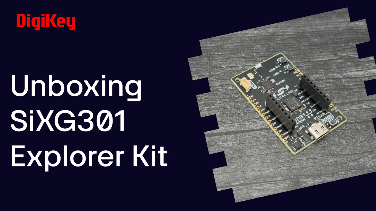
The SixG301 Explorer Kit (SIXG301-EK2719A) (Figure 6) USB-powered development platform provides designers with a compact, low-cost entry point. Built around a SiMG301 module with 4 Mbytes of flash and 512 Kbytes of RAM, this board provides sockets and connectors for add-on sensors and peripherals. An onboard J-Link debugger with a virtual COM port and packet trace interface lets designers perform firmware development and radio evaluation without additional equipment.
 Figure 6: The SIXG301-EK2719A provides a compact, USB-powered development platform with connectors and an onboard J-Link debugger for rapid prototyping. (Image source: Silicon Labs)
For more advanced development and detailed performance characterization, the SixG301 Flash Pro Kit (SIXG301-PK6037A) (Figure 7) combines the SI-MB4002A BRD4002A Wireless Pro Kit Mainboard with a SIXG301-RB4407A plug-in radio board with 4 Mbytes of flash, or a SIXG301-RB4408A plug-in radio board with 8 Mbytes of flash. The mainboard provides integrated debugging, advanced energy monitoring, and a comprehensive peripheral breakout for system-level integration testing, while both plug-in radio boards include a SiMG301 with 512 Kbytes of RAM, a matching network, and a printed circuit board (pc board) antenna.
 Figure 7: The SixG301 Flash Pro Kit combines a feature-rich mainboard with a plug-in radio board and ports for debug and performance characterization. (Image source: Silicon Labs)
The SixG301 Explorer Kit and SixG301 Flash Pro Kit both work with Silicon Labs' Simplicity Studio development environment, which provides configuration wizards, example projects, and access to the Simplicity Software Development Kit (SDK). Together, these resources help designers move efficiently from initial evaluation through prototyping to production-ready designs.
Conclusion
Designers of line-powered smart devices for LED lighting, smart plugs, and switches face mounting pressure to deliver high performance, reliability, multiprotocol connectivity, robust security, and energy efficiency at minimal cost. The Silicon Labs SiMG301 and SiBG301 next-generation Series 3 wireless SoCs, along with their associated development tools, support these requirements and provide a scalable foundation for rapid development.
Disclaimer: The opinions, beliefs, and viewpoints expressed by the various authors and/or forum participants on this website do not necessarily reflect the opinions, beliefs, and viewpoints of DigiKey or official policies of DigiKey.